Function Block Diagram Specifications
Function Block Specifications
| Function Block Specifications | ||||
|---|---|---|---|---|
| Function Block | Specification | Note | ||
| Project | Maximum Registered Function Blocks | 128 | User Library | |
| Maximum Used Function Blocks | Up to CPU memory | |||
| Language | Instruction List Ladder Diagram | |||
| Function Block | Name | 32 characters | ||
| Password | 16 characters | |||
| Password Hint | 40 characters | |||
| Program Capacity | 512 Steps | |||
| Description | 64 characters | |||
| Variable | Maximum Number | 128 | ||
| Input + I/O: 64 Output + I/O: 64 Local Variable: 896 WORDs | Local Variable: Z data register | |||
| Name | 16 characters | |||
| Description | 16 characters | |||
| Version | CICON | v6.00 or higher | ||
| PLC CPU | Multiple Function Blocks | v6.00 or higher | Multiple Function Blocks used | |
| Single Function Block | Any | Single Function Block used | ||
-
IO Variable Limitation:
- For non-Multiple Function Blocks, the number of I/O variables is limited to a maximum of 32.
-
Local (Internal) Variable Usage - Z Data Register:
- For FB Extension, local variables can be assigned to the Z data register.
- The allowable address range for these local variables is from Z128 ~ Z1023.
- The addresses Z0 ~ Z127 are reserved by default for controlling function blocks and cannot be assigned as local variables.
- Using these reserved addresses may lead to improper functioning of the function blocks.
- For FB Extension, local variables can be assigned to the Z data register.
Required CPU
| Required CPU for Function Block | |||
|---|---|---|---|
| PLC Series | CPU | Function Block | Function Block Extension |
| CM1 | XPnA | ✓ | - |
| XPnB | ✓ | ✓ | |
| CPnA ~ D | ✓ | - | |
| CM2 | BP | ✓ | - |
| CM3 | Plus | ✓ | ✓ |
| Mini Modular | ✓ | ✓ | |
| Micro-S | ✓ | ✓ | |
| Pro | ✓ | ✓ | |
-
Function Block (FB) Compatibility with CP Series:
- To utilize Function Blocks (FB) in the CP series, the CPU firmware must be version 4.43 or higher.
-
Support for Multiple Function Blocks:
- Multiple Function Blocks are supported starting from CPU firmware version 6.00 or higher.
-
Definition of Multiple Function Blocks:
- Multiple Function Blocks allow the use of more than one Function Block on a single rung in a program.
Function Block Size
Function Block Download Options
When using Function Blocks in a scan program, the size of the project file increases depending on the number of data registers, variables, and descriptions involved. The Function Block is added to the project file during the compilation process, which may result in differences between the project file size and the step count downloaded to the PLC.
To optimize PLC memory usage, the "FB Information - Full Download" option is disabled by default in the CICON options menu. This typically reduces the size of the download by 50%-80%.

- Left-click Tools and left-click Options.
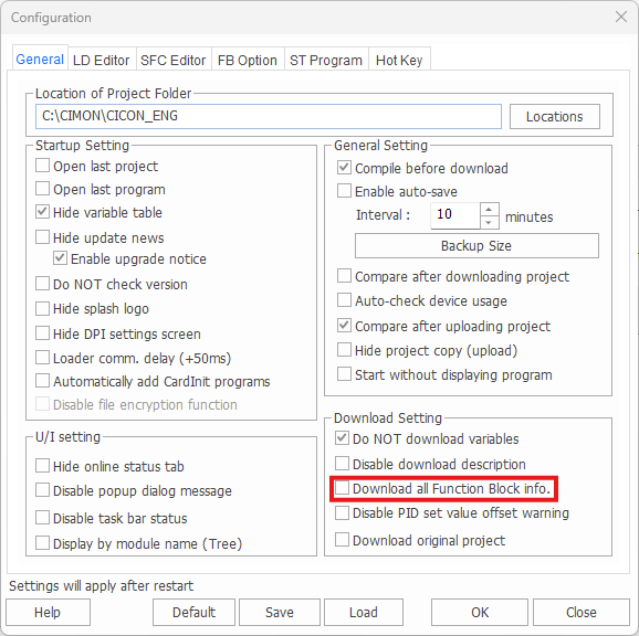
- Under the General tab, check Download all Function Block info.

- Acknowledge the warning and left-click OK.
Full Download Enabled
When the FB Information - Full Download option is enabled, the following data is downloaded to the CPU module:
- Function Block Information:
- Name
- Password
- Hint
- Description
- Function Block Variables:
- Variable Name
- IO
- Type
- Device
- Description
- Scan Program for the Function Block
- Additional Steps (approximately 2–3 steps)
Full Download Disabled
When FB Information - Full Download is disabled, the following data is downloaded to the CPU module:
- Function Block Information:
- Password
- Function Block Variables:
- IO
- Type
- Device
- Scan Program for the Function Block
- Additional Steps (approximately 2–3 steps)
Function Block Upload
When uploading a program from the PLC to CICON, the opened project file in CICON must match the uploaded Function Blocks to ensure consistency. If the Function Blocks in the project file and the uploaded program differ, the variable names and descriptions in the uploaded Function Blocks may differ.
-
When the project file contains the same Function Blocks as the uploaded program:
- If the timestamp is identical, the same Function Blocks are uploaded.
- If the timestamp differs, choose to overwrite the uploaded Function Blocks into the project file.
-
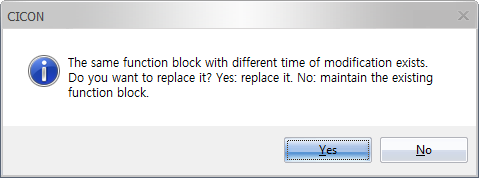
- Upon selecting Yes, a list of available Function Blocks will appear:
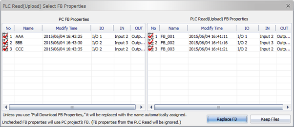
- Replace FB:
- The uploaded Function Block will replace the existing one in the project file.
- Replace FB:
Recovering Overwritten Function Blocks
Even if incorrect Function Blocks are overwritten, recovery is still possible.
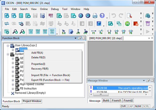
- Right-click the Function Block.
- Choose Recovery FB (R) from the context menu.
- Select the desired Function Block to recover.
Function Block L Data Register
When a Function Block is created, 16 WORDs (256 bits) are automatically assigned to an L data register address. As a result, these specific L addresses cannot be utilized in other scan programs.
| L Data Register Allocation | ||||
|---|---|---|---|---|
| PLC Series | CPU | Input (64 Bit) | Output (64 Bit) | Monitoring |
| CM1 | XP1A | L984.0 ~ L987.F | L988.0 ~ L991.F | L992.0 ~ L999.F |
| XP2A | ||||
| XP3A | L112.0 ~ L115.F | L116.0 ~ L119.F | L120.0 ~ L127.F | |
| CP3 | ||||
| CP4 | ||||
| XP1B | L984.0 ~ L987.F | L988.0 ~ L991.F | L992.0 ~ L999.F | |
| XP2B | ||||
| XP3B | ||||
| CM2 | BP | L48.0 ~ L51.F | L52.0 ~ L55.F | L56.0 ~ L63.F |
| CM3 | Plus | L240.0 ~ L243.F | L244.0 ~ L247.F | L248.0 ~ L255.F |
| Mini Modular | ||||
| Micro-S | ||||
| Pro | ||||
Limitation of Function Block Diagram
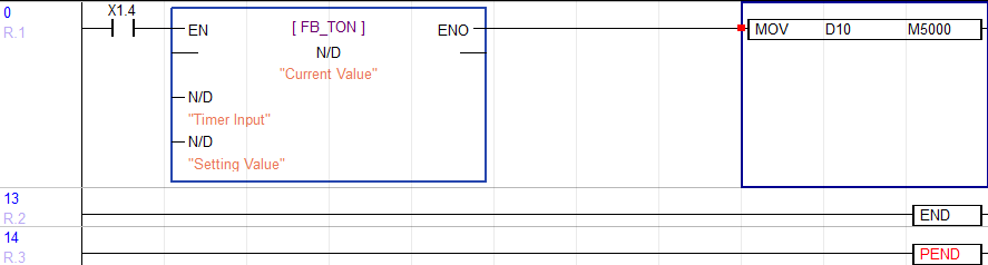
Positive/Negative Transition-Sensing Contacts
When positive and negative transition-sensing (one-shot) contacts are repeatedly used within a Function Block, the Function Block may fail to recognize them. To avoid this issue, replace these transition contacts with a normally open contact:
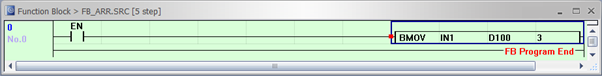
Array Type Instruction
In a Function Block, input and output variables utilize data register addresses sequentially.
For example, if the BMOV instruction is used with the intention of transferring D10, D11, and D12 to D100, D101, and D102 in sequence, the output may not appear as expected. Instead, it could result in a mismatch due to the sequential addressing within the Function Block.
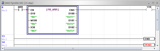

D10 moves to D100, M100 moves to D101, and X30 moves to D102.
Use Index register as below:
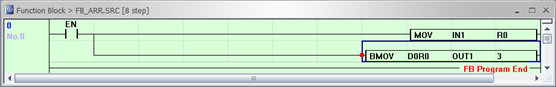
Write an offset value 10 to IN1 (D data register) and make it index register (R0) to have value in sequence.

Timer & Counter
To use a timer or counter in a Function Block, the index register, offset R data register, must be used. Timer and counter instructions can only use the timer and counter data registers.
The index register, R, can be used with the below CPU types:
| R Data Register Compatibility | |
|---|---|
| CPU Type | Minimum Firmware Version |
| XPnB | Version 6.10 |
| XPnE | Any |
| CPnE | Any |
| Plus | Version 6.10 |
| Mini Modular | Version 6.10 |
| Micro-S | Version 6.10 |
| Pro | Version 6.10 |
Timer: TON (On Delay Timer)
Variable Configuration
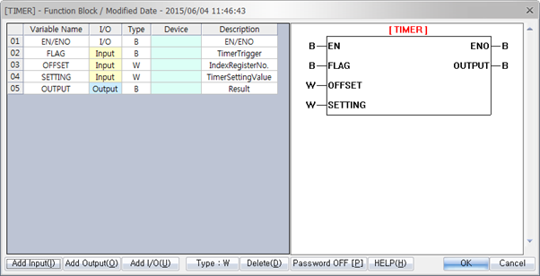
| TON | |||
|---|---|---|---|
| Variable Name | I/O | Type | Device |
| FLAG | Input | BOOL | Operating bit for ON delay timer |
| OFFSET | Input | WORD | Write index register number (0 ~ 15) |
| SETTING | Input | WORD | Write timer set value (TS) (According to PLC parameter, 100ms / 10ms) |
| OUTPUT | Output | BOOL | ON if the FLAG bit remains ON during setting time |
- SETTING : If it is 100 milliseconds and 30 is written, it will be 3 seconds.
Function Block Scan Program
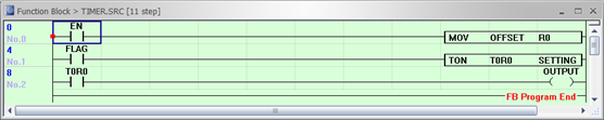
- Before using the index register (R), save the OFFSET value into the register.
- Assign the OFFSET variable value to R0.
- When the ON delay timer is turned ON, the timer begins counting.
- If the timer remains ON for the specified duration set in the SETTING parameter, the OUTPUT will be turned ON.
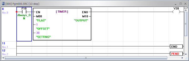
Timer in Scan Program

When using a timer in a Function Block, it is recommended to utilize the F1.0 internal relay flag to handle ON delay or OFF delay functionality.
For example:
- If M0.0 remains ON for 3 seconds (using a 100ms timer), the output M1.0 will be turned ON.
Monitoring
Once a Function Block is downloaded to the CPU and the CPU enters RUN mode, the Function Block appears in monitoring mode.
If M0.0 is OFF, the timer will not function even if the Function Block is running.
When M0.0 is turned ON and remains ON for 3 seconds (using a 100ms timer), the OUTPUT (M1.0) will turn ON.
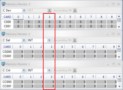
The Timer data register is shown below:
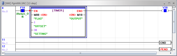
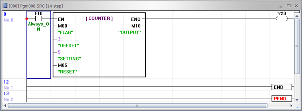
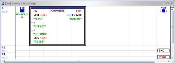
Counter: CTU (Up Counter)
Variable Configuration
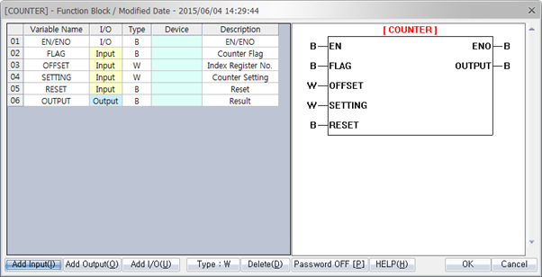
| CTU | |||
|---|---|---|---|
| Variable Name | I/O | Type | Device |
| FLAG | Input | BOOL | Operating bit for up counter |
| OFFSET | Input | WORD | Write index register number (0 ~ 15) |
| SETTING | Input | WORD | Write counter set value (CS) |
| RESET | Input | BOOL | Counter reset bit |
| OUTPUT | Output | BOOL | ON if the FLAG bit is turned ON or OFF as a setting counter |
-RESET: COUNTER is not cleared automatically. It must be cleared by the RESET bit.
Function Block Scan Program
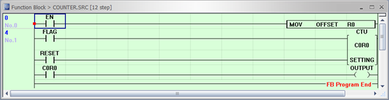
- Before using the index register (R), ensure the OFFSET value is saved in the register.
- Assign the OFFSET variable value to R0.
- When the up counter is turned ON, the counter value increases.
- If the RESET bit is ON, the counter value is cleared.
- Once the counter reaches the assigned value in the SETTING parameter and the condition is met, the OUTPUT will turn ON.
Counter in Scan Program
For Counter operations in a Function Block, the F1.0 internal relay flag is recommended for ON delay or OFF delay functionality.
For example:
- If M0.0 is turned ON and OFF five times (with the OUTPUT activating on the 5th ON event), the output M1.0 will turn ON.
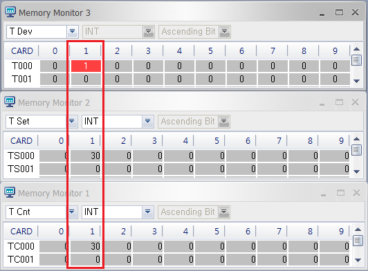
Monitoring
After downloading a Function Block to the CPU and switching it to RUN mode, the Function Block enters monitoring mode.
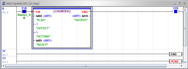
If M0.0 is OFF, the counter will not function even if the Function Block is active.
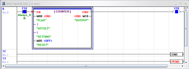
On the 5th ON event of M0.0, the OUTPUT (M1.0) will turn ON.
The Counter data register is shown below:
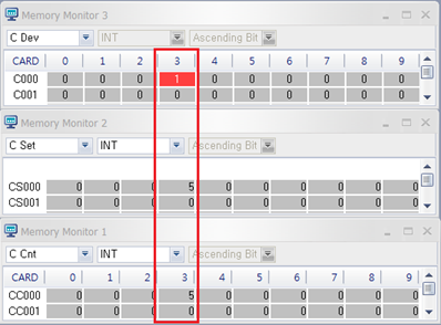
If the RESET bit (M0.5) is turned ON, the counter value is cleared.
After being cleared, the counter data register is shown below: