CM3 DA Module Internal I/O Table
CM3-SP04EOAI & CM3-SP04EOAV Internal I/O Table
| CM3-SP04EOAI & CM3-SP04EOAV Internal I/O Signal Table | |||
|---|---|---|---|
| Direction of Signal CM3-SP04EOAI or CM3-SP04EOAV → CPU | Direction of Signal CPU → CM3-SP04EOAI or CM3-SP04EOAV | ||
| Input | Name of Signal | Output | Name of Signal |
| Xn.0 | DA Module Ready | Yn.0 | Reserved |
| Xn.1 | Reserved | Yn.1 | |
| Xn.2 | Flag indicating the operation condition set up | Yn.2 | Requesting to set up an operation condition |
| Xn.3 | Channel 1 Output Enable (Status) | Yn.3 | Channel 1 Output Enable (Control Command) |
| Xn.3 | Channel 2 Output Enable (Status) | Yn.3 | Channel 2 Output Enable (Control Command) |
| Xn.3 | Channel 3 Output Enable (Status) | Yn.3 | Channel 3 Output Enable (Control Command) |
| Xn.3 | Channel 4 Output Enable (Status) | Yn.3 | Channel 4 Output Enable (Control Command) |
| Xn.7 | Reserved | Yn.7 | Reserved |
| Xn.8 | Yn.8 | ||
| Xn.9 | Yn.9 | ||
| Xn.A | Yn.A | ||
| Xn.B | Yn.B | ||
| Xn.C | Yn.C | ||
| Xn.D | Yn.D | ||
| Xn.E | Yn.E | ||
| Xn.F | DA Module Error Flag | Yn.F | Requesting to Clear Error Flag |
Xn.2 and Yn.2: These flags are used to save an operating condition in the buffer memory into the flash memory of the module permanently.
Output Enable: This is used to output a DA conversion signal based on the assigned channel.
Allocation Example
CM3-SP04EOAI
The CM3-SP04EOAI (current) is allocated one WORD of X (Xn.0 ~ Xn.F) and one WORD of Y (Yn.0 ~ Yn.F).
n is a number representing the CM3-SP04EOAI's position within the chassis.
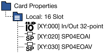
To access the X memory registers for the CM3-SP04EOAI, the X value range is X2.0 ~ X2.F.
To access the Y memory registers for the CM3-SP04EOAI, the Y value range is Y2.0 ~ Y2.F.
CM3-SP04EOAV
The CM3-SP04EOAV (voltage) is allocated one WORD of X (Xn.0 ~ Xn.F) and one WORD of Y (Yn.0 ~ Yn.F).
n is a number representing the CM3-SP04EOAV's position within the chassis.
To access the X memory registers for the CM3-SP04EOAV, the X value range is X3.0 ~ X3.F.
To access the Y memory registers for the CM3-SP04EOAV, the Y value range is Y3.0 ~ Y3.F.