CM3 Positioning Module Internal I/O Table
CM3-SP02POS Internal I/O Table
| CM3-SP02POS Internal I/O Table | |||
|---|---|---|---|
| Direction of Signal CM3-SP02POS → CPU | Direction of Signal CPU → CM3-SP02POS | ||
| Input | Name of Signal | Output | Name of Signal |
| Xn.0 | Positioning Module Ready | Yn.0 | CPU Ready |
| Xn.1 | Error | Yn.1 | Reserved |
| Xn.2 | Reserved | Yn.2 | |
| Xn.3 | Yn.3 | ||
| Xn.4 | Axis 1 Command ACK | Yn.4 | Axis 1 Positioning Start |
| Xn.5 | Axis 1 Busy | Yn.5 | Axis 1 MPG Run |
| Xn.6 | Axis 1 Error | Yn.6 | Axis 1 Forward JOG |
| Xn.7 | Axis 1 Positioning Complete | Yn.7 | Axis 1 Reverse JOG |
| Xn.8 | Axis 1 M Code ON | Yn.8 | Axis 1 Stop |
| Xn.9 | Reserved | Yn.9 | Reserved |
| Xn.A | Axis 2 Command ACK | Yn.A | Axis 2 Positioning Start |
| Xn.B | Axis 2 Busy | Yn.B | Axis 2 MPG Run |
| Xn.C | Axis 2 Error | Yn.C | Axis 2 Forward JOG |
| Xn.D | Axis 2 Positioning Complete | Yn.D | Axis 2 Reverse JOG |
| Xn.E | Axis 2 M Code ON | Yn.E | Axis 2 Stop |
| Xn.F | Reserved | Yn.F | Reserved |
Allocation Example
The CM3-SP02POS module is allocated one WORD of X (Xn.0 ~ Xn.F) and one WORD of Y (Yn.0 ~ Yn.F).
n is a number representing the CM3-SP02POS module's position within the chassis.
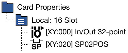
To access the X memory registers for this CM3-SP02POS example, the X value range is X2.0 ~ X2.F.
To access the Y memory registers for this CM3-SP02POS example, the Y value range is Y2.0 ~ Y2.F.
Input Signal Specifications
| Input Signal Specifications | ||||
|---|---|---|---|---|
| Signal | Rated Input Voltage/Current | Working Voltage Range | ON Voltage/Current | OFF Voltage/Current |
| Point DOG | DC 24V 5mA | DC 19.2V ~ 26.4V | DC 19V 4mA or more | DC 11V 1mA |
| External High Limit (HL) | ||||
| External Low Limit (LL) | ||||
| Drive Ready (RDY) | ||||
| Inposition (INP) | ||||
| MPG Phase A (MPG A+ | MPG A-) MPG Phase B (MPG B+ | MPG B-) | DC 5V 7mA | DC 4.25V ~ 5.5V | DC 2.5V 3mA or more | DC 1V 1mA or less |
  | ||||
| HOME (ZERO05) (ZERO25) | DC 5V 7mA | DC 4.25V ~ 5.5V | DC 2.5V 3mA or more | DC 1V 1mA |
| DC 24V 5mA | DC 19.2V ~ 26.4V | DC 19V 4mA or more | DC 11V 1mA | |
 | ||||
Output Signal Specifications
| Output Signal Specifications | |||||||||||||||||||||||||||||||||
|---|---|---|---|---|---|---|---|---|---|---|---|---|---|---|---|---|---|---|---|---|---|---|---|---|---|---|---|---|---|---|---|---|---|
| Signal | Rated Voltage | Working Voltage | Maximum Current Inrush Current | Voltage Drop at ON | Leakage Current at OFF | ||||||||||||||||||||||||||||
| Pulse Output (RP) |
| ||||||||||||||||||||||||||||||||
| Pulse Output (FP) | DC 5V ~ 24V | DC 4.75V ~ 26.4V | 50mA per point 0.2A (10ms or less) | DC 0.5V | 0.1mA or less | ||||||||||||||||||||||||||||
| Deviation Counter Clear (CLEAR) | DC 5V ~ 24V | DC 4.75V ~ 26.4V | 0.1A per point 0.4A (10ms or less) | DC 1V | 0.1mA or less | ||||||||||||||||||||||||||||


