CM3 Thermocouple Module Internal I/O Table
CM3-SP04ETO Internal I/O Table
| CM3-SP04ETO Internal I/O Signal Table | |||
|---|---|---|---|
| Direction of Signal CM3-SP04ETO → CPU | Direction of Signal CPU → CM3-SP04ETO | ||
| Input | Name of Signal | Output | Name of Signal |
| Xn.0 | TC Module Ready | Yn.0 | Reserved |
| Xn.1 | TC conversion completion flag | Yn.1 | |
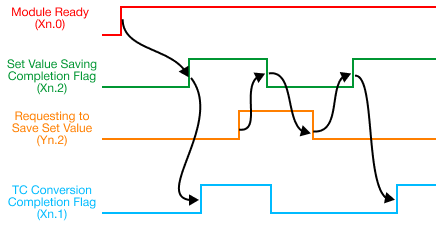
| Xn.2 | Set value saving completion flag | Yn.2 | Requesting to save set value |
| Xn.3 | Reserved | Yn.3 | Reserved |
| Xn.4 | Yn.4 | ||
| Xn.5 | Yn.5 | ||
| Xn.6 | Yn.6 | ||
| Xn.7 | Yn.7 | ||
| Xn.8 | Yn.8 | ||
| Xn.9 | Yn.9 | ||
| Xn.A | Yn.A | ||
| Xn.B | Yn.B | ||
| Xn.C | Yn.C | ||
| Xn.D | Yn.D | ||
| Xn.E | Yn.E | ||
| Xn.F | TC Module Error Flag> | Yn.F | Requesting to Clear Error Flag |
Input Signal
| Input Signal | ||
|---|---|---|
| Data Register | Signal Name | Description |
| Xn.0 | TC Module Ready | This signal is turned ON at the time TC conversion is completely ready (CPU power is ON). |
| Xn.1 | TC conversion completion flag |
|
| Xn.2 | Set value saving completion flag |
|
| Xn.F | TC module error flag |
|

Output Signal
| Output Signal | ||
|---|---|---|
| Data Register | Signal Name | Description |
| Yn.2 | Requesting to save set value |
|
| Yn.F | Requesting to clear error |
|
Allocation Example
The CM3-SP04ETO is allocated one WORD of X (Xn.0 ~ Xn.F) and one WORD of Y (Yn.0 ~ Yn.F).
n is a number representing the CM3-SP04ETO's position within the chassis.
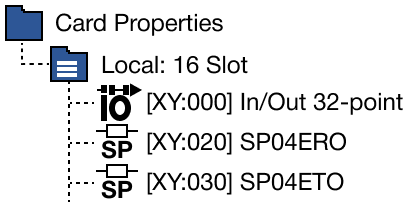
To access the X memory registers for this CM3-SP04ETO example, the X value range is X3.0 ~ X3.F.
To access the Y memory registers for this CM3-SP04ETO example, the Y value range is Y3.0 ~ Y3.F.