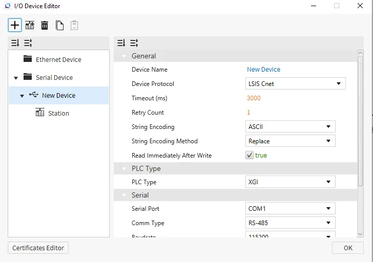
Canvas supports LSIS Cnet as a way to connect to devices that support this protocol. There are no additional configuration options.
- General Format: %[Device Name][Data Type][Address Number]
-
Data Type | Symbol | # of Bits |
|---|
| BIT | X | 1 |
| BYTE | B | 8 |
| WORD | W | 16 |
| DWORD | D | 32 |
| QWORD | L | 64 |
- This is also true for I/Q and U device formats.
Address Number: denoted in the specified data type.
- Example: if
B is used, Address Number 5 represents the 6th byte in the memory area (0-based index).
- Example: if
L is used, Address Number 16 represents the 17th QWORD in the memory area (0-based index).
- Example: the address %MB016 represents the 17th byte of the M memory area. This same starting address is pointed to using %MX128, %MW008, %MD004, or %ML002.
- Gateway will automatically convert the provided address into
BYTE notation, unless it was specified by BIT notation. This is done to allow for continuous memory blocks to be read in a single request.
- I/Q Device Format: %[Device Name][Data Type][Base Number].[Slot Number].[Module Number]
Base Number: Range of 0 ~ 127, represented in decimal notation.Slot Number: Range of 0 ~ 15, represented in decimal notation.Module Number: similar to Address Number in the generic format, where it is in the form of the Data Type.
- U Device Format: %[Device Name][Data Type][Base Number].[Slot Number].[Channel Number]
Base Number: Range of 0 ~ 7, represented in decimal notation.Slot Number: Range of 0 ~ 15, represented in decimal notation.Channel Number: similar to Address Number in the generic format, where it is in the form of the Data Type.
| Device | Symbol | Bit Address | BYTE Address | WORD Address | DWORD Address | QWORD Address | Access |
|---|
| Input Points | I | %IX000.00.00 - %IX127.15.63 | %IB000.00.0 - %IB127.15.7 | %IW000.00.0 - %IW127.15.3 | %ID000.00.0 - %ID127.15.1 | %IL000.00.0 - %IL127.15.0 | R/W |
| Output Points | Q | %QX000.00.00 - %QX127.15.63 | %QB000.00.0 - %QB127.15.7 | %QW000.00.0 - %QW127.15.3 | %QD000.00.0 - %QD127.15.1 | %QL000.00.0 - %QL127.15.0 | R/W |
| Automatic Variable | A | %AX0000000 - %AX8388607 | %AB0000000 - %AB1048575 | %AW000000 - %AW524287 | %AD000000 - %AD262143 | %AL000000 - %AL131071 | R/W |
| Direct Variable | M | %MX0000000 - %MX4194303 | %MB000000 - %MB524287 | %MW000000 - %MW262143 | %MD000000 - %MD131071 | %ML00000 - %ML65535 | R/W |
| Direct Variable | R | %RX000000 - %RX524287 | %RB00000 - %RB65535 | %RW00000 - %RW32767 | %RD00000 - %RD16383 | %RL0000 - %RL8191 | R/W |
| Direct Variable | W | %WX0000000 - %WX8388607 | %WB0000000 - %WB1048575 | %WW000000 - %WW524287 | %WD000000 - %WD262143 | %WL000000 - %WL131071 | R/W |
| System Flag | F | %FX00000 - %FX65535 | %FB0000 - %FB8191 | %FW0000 - %FW4095 | %FD0000 - %FD2047 | %FL0000 - %FL1023 | R |
| PID Flag | K | %KX000000 - %KX134399 | %KB0000 - %KB16799 | %KW0000 - %KW8399 | %KD0000 - %KD4299 | %KL0000 - %KL2199 | R/W |
| HS Link Flag | L | %LX000000 - %LX180223 | %LB00000 - %LB22527 | %LW00000 - %LW11263 | %LD0000 - %LD5631 | %LL0000 - %LL2815 | R/W |
| Analog Refresh Flag | U | %UX0.00.000 - %UX7.15.511 | %UB0.00.00 - %UB7.15.63 | %UW0.00.00 - %UW7.15.31 | %UD0.00.00 - %UD7.15.15 | %UL0.00.00 - %UL7.15.7 | R/W |
| P2P Parameters Flag | N | %NX000000 - %NX401407 | %NB00000 - %NB50175 | %NW00000 - %NW25087 | %ND00000 - %ND12543 | %NL0000 - %NL6271 | R/W |
- General Format: [Device Name][Address Number]
- For devices that support both bit and WORD formats, the difference is the inclusion of a bit number (in Hexadecimal notation) as the last character in the address.
- If the device only supports bit addressing, then this bit number is not used (
T and C devices).
- U Device Format: [Device Name][Base Number].[Slot Number].[Special Module Inner WORD Number]
Base Number: Range of 0 ~ 7, represented in decimal notation.Slot Number: Range of 0 ~ F, represented in Hexadecimal notation.Special Module Inner WORD Number: Range of 0 ~ 31, represented in decimal notation.
| Device | Symbol | Bit Address | WORD Address | Access |
|---|
| Input / Output Relay | P | P00000 - P2047F | P0000 - P2047 | R/W |
| Auxiliary Relay | M | M00000 - M2047F | M0000 - M2047 | R/W |
| Keep Relay | K | K00000 - K4095F | K0000 - K4095 | R/W |
| Link Relay | L | L000000 - L11263F | L00000 - L11263 | R/W |
| Special Relay | F | F00000 - F2047F | F0000 - F2047 | R |
| Timer - Contact | T | T0000 - T2047 | - | R/W |
| Counter - Contact | C | C0000 - C2047 | - | R/W |
| Timer - Current Value | T | - | T0000 - T2047 | R/W |
| Counter - Current Value | C | - | C0000 - C2047 | R/W |
| Data Register | D | - | D00000 - D32767 | R/W |
| Special Module Register | U | - | U00.00 - U7F.31 | R/W |
| Index Register | Z | - | Z000 - Z127 | R/W |
| Communication Data Register | N | - | N00000 - N21503 | R/W |
| File Register | R | - | R00000 - R32767 | R/W |
| File Register | ZR | - | ZR00000 - ZR65535 | R/W |
| Device | Symbol | Bit Address | WORD Address | Access |
|---|
| Input / Output Relay | P | P00000 - P4095F | P0000 - P4095 | R/W |
| Auxiliary Relay | M | M00000 - M4095F | M0000 - M4095 | R/W |
| Keep Relay | K | K00000 - K4095F | K0000 - K4095 | R/W |
| Link Relay | L | L000000 - L11263F | L00000 - L11263 | R/W |
| Special Relay | F | F00000 - F4095F | F0000 - F4095 | R |
| Timer - Contact | T | T0000 - T8191 | - | R/W |
| Counter - Contact | C | C0000 - C4095 | - | R/W |
| Timer - Current Value | T | - | T0000 - T8191 | R/W |
| Counter - Current Value | C | - | C0000 - C4095 | R/W |
| Step Controller | S | - | S000 - S255 | R/W |
| Data Register | D | - | D000000 - D524287 | R/W |
| Special Module Register | U | - | U00.00 - U7F.31 | R/W |
| Index Register | Z | - | Z000 - Z255 | R/W |
| Communication Data Register | N | - | N00000 - N21503 | R/W |
| File Register | R | - | R00000 - R32767 | R/W |
| File Register | ZR | - | ZR000000 - ZR524287 | R/W |