CM3 HSC Module Internal I/O Table
CM3-SP02HSC & CM3-SP02HSD Internal I/O Table
Input Signals
| Input Signals | |||
|---|---|---|---|
| Data Register Number | Signal Name | Description | |
| Channel 1 | Channel 2 | ||
| Xn.0 | Xn.F | DPRAM ACK |
|
| Xn.1 | Xn.8 | Counted Value Greater 1 |
|
| Xn.2 | Xn.9 | Counted Value Coincident 1 |
|
| Xn.3 | Xn.A | Counted Value Less 1 |
|
| Xn.4 | Xn.B | Detect Request for Outer Presetting |
|
| Xn.5 | Xn.C | Counted Value Greater 2 |
|
| Xn.6 | Xn.D | Counted Value Coincident 2 |
|
| Xn.7 | Xn.E | Counted Value Less 2 |
|
Output Signals
| Output Signals | ||||
|---|---|---|---|---|
| Data Register Number | Signal Name | Operation Timing | Description | |
| Channel 1 | Channel 2 | |||
| Yn.0 | Yn.8 | Requesting to Reset Coincidence Signal 1 |
| |
| Yn.1 | Yn.9 | Requesting to Preset |
| |
| Yn.2 | Yn.A | Enable Coincidence Output |
| |
| Yn.3 | Yn.B | Request DPRAM |
| |
 | ||||
| Yn.4 | Yn.C | Enable Count |
| |
| Yn.5 | Yn.D | Requesting to Reset Detect Outer Presetting |
| |
| Yn.6 | Yn.E | Requesting to Start Counting |
| |
| ||||
| Yn.7 | Yn.F | Requesting to Reset Coincidence Signal 2 |
| |
Allocation Example
CM3-SP02HSC
The CM3-SP02HSC is allocated one WORD of X (Xn.0 ~ Xn.F) and one WORD of Y (Yn.0 ~ Yn.F).
n is a number representing the CM3-SP02HSC's position within the chassis.
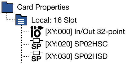
To access the X memory registers for this CM3-SP02HSC example, the X value range is X2.0 ~ X2.F.
To access the Y memory registers for this CM3-SP02HSC example, the Y value range is Y2.0 ~ Y2.F.
CM3-SP02HSD
The CM3-SP02HSD is allocated one WORD of X (Xn.0 ~ Xn.F) and one WORD of Y (Yn.0 ~ Yn.F).
n is a number representing the CM3-SP02HSD's position within the chassis.
To access the X memory registers for this CM3-SP02HSD example, the X value range is X3.0 ~ X3.F.
To access the Y memory registers for this CM3-SP02HSD example, the Y value range is Y3.0 ~ Y3.F.