Serial Device Communication
Communication Cable Wiring
Please refer to the below tables for the Xpanel serial port wiring:
For the RS-232C ports, Xpanel provides the standard DB9 RS-232C pin assignment.
eXT04+ & nXT07
- The below serial port is applicable to the following Xpanel models:
- eXT04
- eXT07
- nXT07
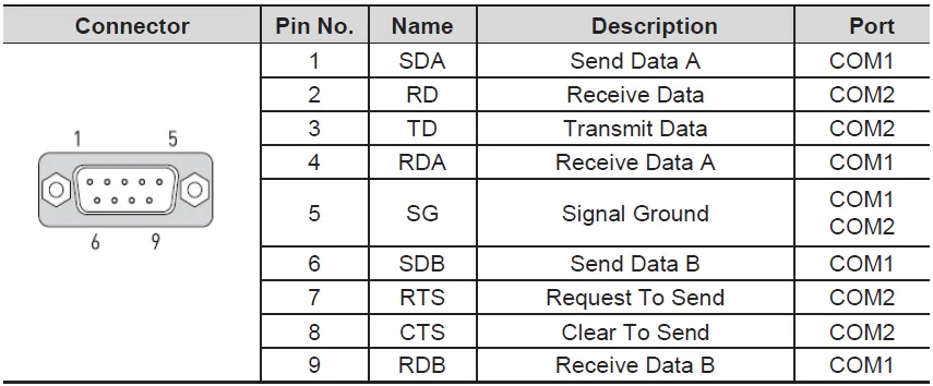
- Use COM1 for RS-422/485
- Use COM2 for RS-232C
eXT10+ and eXT2
- The below serial ports are applicable to the following Xpanel models:
- eXT10
- eXT12
- eXT15
- eXT2-07
- eXT2-10
- eXT2-12
- eXT2-15
COM1
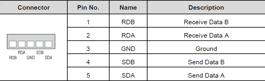
- Use COM1 for RS-422/485
COM2
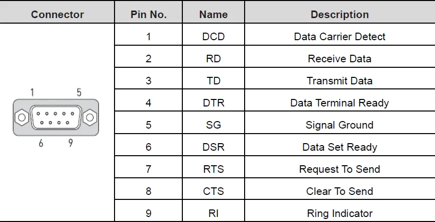
- Use COM2 for RS-232C
COM3
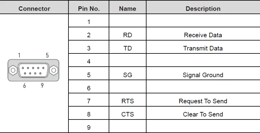
- Use COM3 for RS-232C
Supported Drivers
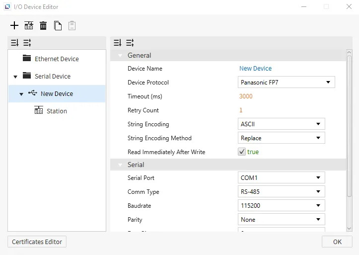
Serial Devices are used when a connection to another device is made via a serial cable. Users will need to input the Serial Port of the device they are connecting to, the Comm Type, and the Baudrate. Users can also select the String Encoding and the String Encoding Method. Users can also change settings such as the Timeout time, Retry Count, and Transmission Delay. Users will also be able to change the name of the Device and the Protocol of the device as well.

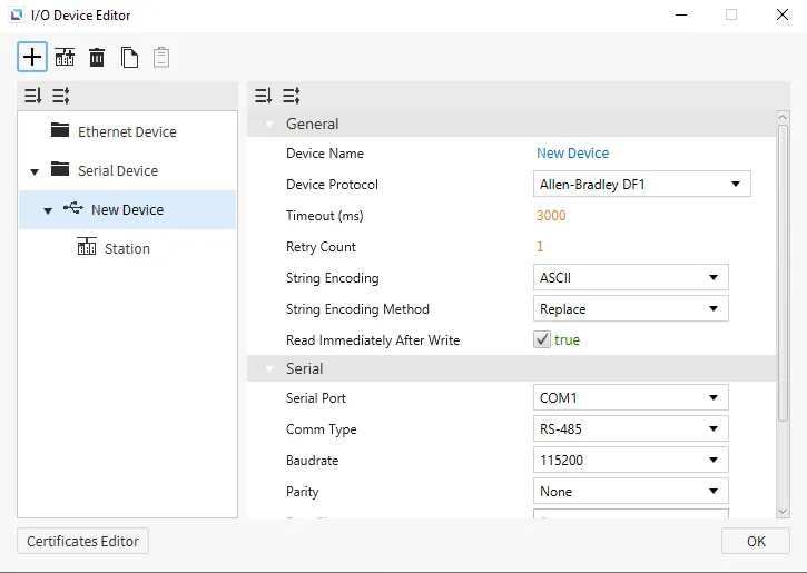
Allen-Bradley DF-1
Canvas supports Allen-Bradley DF-1 as a way to connect to devices that support this protocol. Users will be able to select the Error Detection and Flow Control for the protocol. Users can choose between BCC and CRC for Error Detection, and can turn on, off or control Flow Control. No additional settings will appear after selecting the device.
Memory Area and Ranges
| Memory Area | Symbol | Digital | Analog | Address Notation | Access |
|---|---|---|---|---|---|
| Output Files | O | O:0.0/0 - O:0.30/15 | O:0.0 - O:0.30 | Decimal | R/W |
| Input Files | I | I:0.0/0 - I:0.30/15 | I:0.0 - I:0.30 | Decimal | R |
| Status Files | S | S:0/0 - S:163/15 | S:0 - S:163 | Decimal | R |
| Binary Files | B | B3:0/0 - B3:255/15 B9:0/0 - B255:255/15 | B3:0 - B3:255 B9:0 - B255:255 | Decimal | R/W |
| Integer Files | N | N7:0/0 - N7:255/15 N9:0/0 - N255:255/15 | N7:0 - N7:255 N9:0 - N255:255 | Decimal | R/W |
| Float Files | F | - | F8:0 - F255:255 | Decimal | R/W |
| Long Files | L | - | L9:0 - L255:255 | Decimal | R/W |
| String Files | ST | - | ST9:0 - ST255:255 | Decimal | R/W |
| Timer Files | T | T4:0.0/0 - T4:255.2/15 T9:0.0/0 - T255:255.2/15 | T4:0.0 - T4:255.2 T9:0.0 - T255:255.2 | Decimal | R/W |
| Counter Files | C | C5:0.0/0 - C5:255.2/15 C9:0.0/0 - C255:255.2/15 | C5:0.0 - C5:255.2 C9:0.0 - C255:255.2 | Decimal | R/W |
| Control Files | R | R6:0.0/0 - R6:255.2/15 R9:0.0/0 - R255:255.2/15 | R6:0.0 - R6:255.2 R9:0.0 - R255:255.2 | Decimal | R/W |
Communication Cable Wiring
The 1761-CBL-PM02 cable was used to develop this protocol, and will work when attempting to connect using this protocol.
ATIVA Serial
Canvas supports ATIVA Serial as a way to connect to devices that support this protocol. There are no additional configuration options.

Format
- Analog Tag Format: {Symbol}{Address Number}
- Example: D0 retrieves the full WORD value.
- Digital Tag Format: {Symbol}{Address Number}{Bit Number}
- Example: D0A retrieves the 10th bit value of the WORD D0.
Memory Area and Ranges
| Memory Area | Symbol | Digital | Analog | Access |
|---|---|---|---|---|
| External Input | X | X000.0 - X511.F | X0000 - X5110 | R |
| External Output | Y | Y000.0 - Y511.F | Y0000 - Y5110 | R/W |
| Internal Relay | M | M000.0 - M999.F | M0000 - M9990 | R/W |
| Internal Relay | L | L000.0 - L999.F | L0000 - L9990 | R/W |
| Latch (Non-Volatile) Relay | K | K000.0 - K999.F | K0000 - K9990 | R/W |
| Flags | F | F000.0 - F127.F | F0000 - F1270 | R |
| Timer - Output | T | T0000 - T4095 | - | R/W |
| Timer - Current Value | TC | - | TC0000 - TC4095 | R/W |
| Timer - Set Value | TS | - | TS0000 - TS4095 | R/W |
| Counter - Output | C | C0000 - C4095 | - | R/W |
| Counter - Current Value | CC | - | CC0000 - CC4095 | R/W |
| Counter - Set Value | CS | - | CS0000 - CS4095 | R/W |
| Step Controller | S | - | S00 - S99 | R/W |
| Data Memory | D | D00000.0 - D31999.F | D00000 - D31999 | R/W |
| Index Register | R | - | R00 - R19 | R/W |
| Subroutine | Z | - | Z0000 - Z1029 | R/W |
| Sequential Function Chart | Q | Q000.0 - Q511.F | Q0000 - Q5110 | R/W |
CIMON PLC (HMI Protocol)
This is the default protocol for Canvas. There are no additional configuration options.
Format
- Analog Tag Format: {Symbol}{Address Number}
- Example: D0 retrieves the full WORD value.
- Digital Tag Format: {Symbol}{Address Number}{Bit Number}
- Example: D0A retrieves the 10th bit value of the WORD D0.
Memory Area and Ranges
| Memory Area | Symbol | Digital | Analog | Access |
|---|---|---|---|---|
| External Input | X | X000.0 - X511.F | X0000 - X5110 | R |
| External Output | Y | Y000.0 - Y511.F | Y0000 - Y5110 | R/W |
| Internal Relay | M | M000.0 - M999.F | M0000 - M9990 | R/W |
| Internal Relay | L | L000.0 - L999.F | L0000 - L9990 | R/W |
| Latch (Non-Volatile) Relay | K | K000.0 - K999.F | K0000 - K9990 | R/W |
| Flags | F | F000.0 - F127.F | F0000 - F1270 | R |
| Timer - Output | T | T0000 - T4095 | - | R/W |
| Timer - Current Value | TC | - | TC0000 - TC4095 | R/W |
| Timer - Set Value | TS | - | TS0000 - TS4095 | R/W |
| Counter - Output | C | C0000 - C4095 | - | R/W |
| Counter - Current Value | CC | - | CC0000 - CC4095 | R/W |
| Counter - Set Value | CS | - | CS0000 - CS4095 | R/W |
| Step Controller | S | - | S00 - S99 | R/W |
| Data Memory | D | D00000.0 - D31999.F | D00000 - D31999 | R/W |
| Index Register | R | - | R00 - R19 | R/W |
| Subroutine | Z | - | Z0000 - Z1029 | R/W |
| Sequential Function Chart | Q | Q000.0 - Q511.F | Q0000 - Q5110 | R/W |
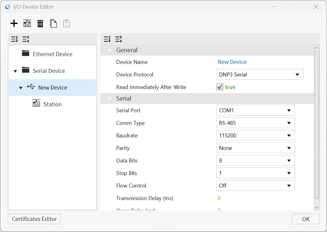
DNP3 Serial
Canvas supports DNP3 Serial as a way to connect to devices that support this protocol. Users can configure the Open Delay.
Format
| Group | Variations | Digital | Analog | Address Notation | Access |
|---|---|---|---|---|---|
| 1: Binary Input | 0: Default Variation 1: Packet Format 2: With Flags | 1.{0, 1, 2}.{0-65535}.{Value, Explicit} | 1.{0, 1 ,2}.{0-65535}.{Flags, Timestamp} | Decimal | R |
| 3: Double Binary Input | 0: Default Variation 1: Packet Format 2: With Flags | - | 3.{0, 1, 2}.{0-65535}.{Value, Explicit, Flags, Timestamp} | Decimal | R |
| 10: Binary Output | 0: Default Variation 1: Packet Format 2: Output Status With Flags | 10.{0, 1, 2}.{0-65535}.{Value, Explicit} | 10.{0, 1, 2}.{0-65535}.{Flags, Timestamp} | Decimal | R/W(Value, Explicit) |
| 20: Counter | 0: Default Variation 1: 32-bit With Flag 2: 16-bit With Flag 5: 32-bit Without Flag 6: 16-bit Without Flag | - | 20.{0, 1, 2, 5, 6}.{0-65535}.{Value, Explicit, Flags, Timestamp} | Decimal | R |
| 21: Frozen Counter | 0: Default Variation 1: 32-bit With Flag 2: 16-bit With Flag 5: 32-bit With Flag and Time 6: 16-bit With Flag and Time 9: 32-bit Without Flag 10: 16-bit Without Flag | - | 21.{0, 1, 2, 5, 6, 9, 10}.{0-65535}.{Value, Explicit, Flags, Timestamp} | Decimal | R |
| 30: Analog Input | 0: Default Variation 1: 32-bit With Flag 2: 16-bit With Flag 3: 32-bit Without Flag 4: 16-bit Without Flag 5: Single-Precision With Flag 6: Double-Precision With Flag | - | 30.{0, 1, 2, 3, 4, 5, 6}.{0-65535}.{Value, Explicit, Flags, Timestamp} | Decimal | R |
| 40: Analog Output | 0: Default Variation 1: 32-bit With Flag 2: 16-bit With Flag 3: Single-Precision With Flag 4: Double-Precision With Flag | - | 40.{0, 1, 2, 3, 4}.{0-65535}.{Value, Explicit, Flags, Timestamp} | Decimal | R/W(Value, Explicit) |
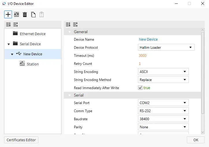
Hallim Loader
Canvas supports Hallim Loader as a way to connect to devices that support this protocol. No additional settings will appear on the selection of this protocol.
Format
- Generic Format: {Device Name}{Address Number}
Device Name: symbol for the memory area being used.Address Number: index of the memory address being requested, represented in decimal notation.
- X, Y, M, L, K, or F Area Format: {Device Name}{Address Number}{Bit Number}
- Some memory areas can be accessed as either an analog or digital tag.
Device Name: symbol for the memory area being used.Address Number: index of the memory address being requested, represented in decimal notation.Bit Number: bit which is being requested, represented in Hexadecimal notation.- For analog tags, the
Bit Numbershould always be 0.
- For analog tags, the
Memory Area and Ranges
| Memory Area | Symbol | Digital | Analog | Access |
|---|---|---|---|---|
| External Input | X | X000.0 - X511.F | X0000 - X5110 | R |
| External Output | Y | Y000.0 - Y511.F | Y0000 - Y5110 | R/W |
| Internal Relay | M | M000.0 - M999.F | M0000 - M9990 | R/W |
| Internal Relay | L | L000.0 - L999.F | L0000 - L9990 | R/W |
| Latch (Non-Volatile) Relay | K | K000.0 - K999.F | K0000 - K9990 | R/W |
| Flags | F | F000.0 - F127.F | F0000 - F1270 | R |
| Timer - Output | T | T0000 - T4095 | - | R/W |
| Timer - Current Value | TC | - | TC0000 - TC4095 | R/W |
| Timer - Set Value | TS | - | TS0000 - TS4095 | R/W |
| Counter - Output | C | C0000 - C4095 | - | R/W |
| Counter - Current Value | CC | - | CC0000 - CC4095 | R/W |
| Counter - Set Value | CS | - | CS0000 - CS4095 | R/W |
| Step Controller | S | - | S00 - S99 | R/W |
| Data Memory | D | D00000.0 - D31999.F | D00000 - D31999 | R/W |
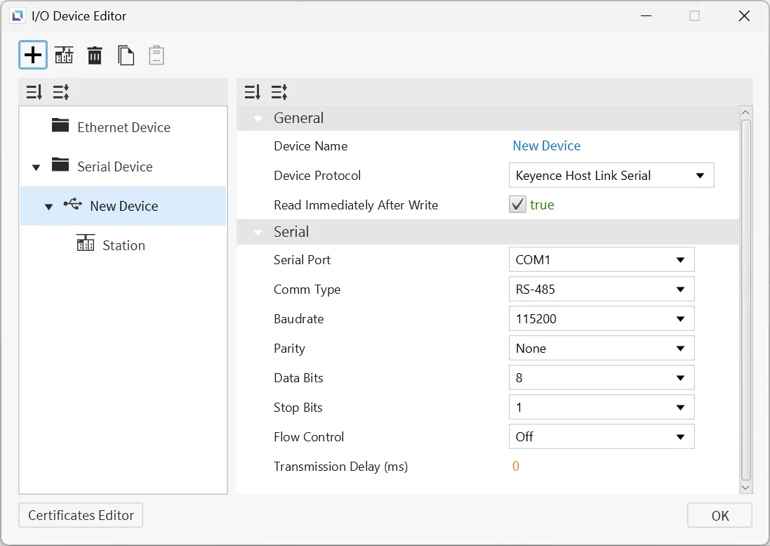
Keyence Host Link Serial
Canvas supports Keyence Host Link Serial as a way to connect to devices that support this protocol. There are no additional configuration options.
Memory Area and Ranges
| Memory Area | Symbol | Digital | Analog | Address Notation | Access |
|---|---|---|---|---|---|
| Relay | R | R0 - R199915 | R0 - R199900 | Decimal | R/W |
| Link Relay | B | B0 - B7FFF | B0 - B7FF0 | Hexadecimal | R/W |
| Internal Auxiliary Relay | MR | MR0 - MR399915 | MR0- MR399900 | Decimal | R/W |
| Latch Relay | LR | LR0 - LR99915 | LR0 - LR99900 | Decimal | R/W |
| Control Relay | CR | CR0 - CR99915 | CR0 - CR99900 | Decimal | R/W |
| Virtual Relay | VB | VB0 - VBF9FF | VB0 - VBF9F0 | Hexadecimal | R/W |
| Data Memory | DM | - | DM0 - DM65535 | Decimal | R/W |
| Extended Data Memory | EM | - | EM0 - EM65535 | Decimal | R/W |
| File Register | FM | - | FM0 - FM524287 | Decimal | R/W |
| File Register (SQ) | ZF | - | ZF0 - ZF524287 | Decimal | R/W |
| Link Register | W | - | W0 - W7FFF | Hexadecimal | R/W |
| Temporary Data Memory | TM | - | TM0 - TM9999 | Decimal | R/W |
| Index Register | Z | - | Z1 - Z12 | Decimal | R/W |
| Timer | T | - | T0 - T9999 | Decimal | R |
| Timer (Current Value) | TC | - | TC0 - TC9999 | Decimal | R/W |
| Timer (Set Value) | TS | - | TS0 - TS9999 | Decimal | R/W |
| Counter | C | - | C0 - C9999 | Decimal | R |
| Counter (Current Value) | CC | - | CC0 - CC9999 | Decimal | R/W |
| Counter (Set Value) | CS | - | CS0 - CS9999 | Decimal | R/W |
| High-Speed Counter | CTH | - | CTH0 - CTH3 | Decimal | R/W |
| High-Speed Counter Comparator | CTC | - | CTC0 - CTC7 | Decimal | R/W |
| Control Memory | CM | - | CM0 - CM65535 | Decimal | R/W |
| Virtual Memory | VM | - | VM0 - VM65535 | Decimal | R/W |
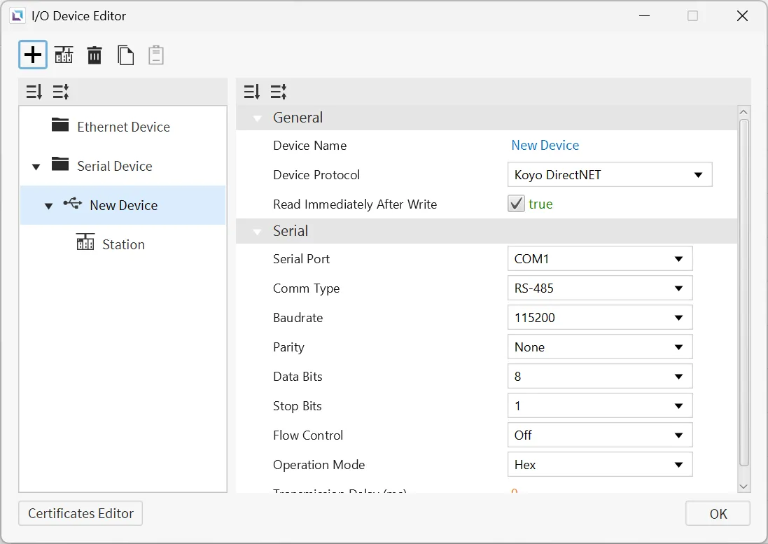
Koyo DirectNET
Canvas supports Koyo DirectNET as a way to connect to devices that support this protocol. Users can configure the Operation Mode.
Memory Area and Ranges
| Memory Area | Symbol | Digital | Analog | Address Notation | Access | Note |
|---|---|---|---|---|---|---|
| Remote Input | GX | GX0 - GX3777 | - | Octal | R/W | - |
| Remote Output | GY | GY0 - GY3777 | - | Octal | R/W | - |
| Input Points | X | X0 - X1777 | - | Octal | R/W | - |
| Output Points | Y | Y0 - Y1777 | - | Octal | R/W | - |
| Control Relays | C | C0 - C3777 | - | Octal | R/W | - |
| Stage Status | S | S0 - S1777 | - | Octal | R/W | - |
| Timer Status | T | T0 - T377 | - | Octal | R/W | - |
| Counter Status | CT | CT0 - CT377 | - | Octal | R/W | - |
| Special Relays | SP | SP0 - SP777 | - | Octal | R/W | - |
| Timer Accumulator | TA | - | TA0 - TA377 | Octal | R/W | - |
| Counter Accumulator | CTA | - | CTA0 - CTA377 | Octal | R/W | - |
| V Memory | V | - | V0 - V77777 | Octal | R/W | 1 WORD (2 bytes) per unit |
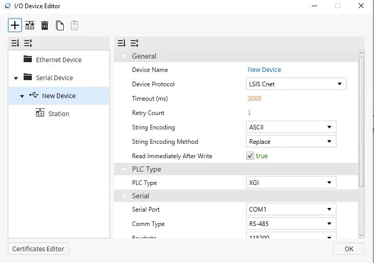
LSIS Cnet
Canvas supports LSIS Cnet as a way to connect to devices that support this protocol. There are no additional configuration options.
XGI
Format
- General Format: %[Device Name][Data Type][Address Number]
-
Data TypeSymbol # of Bits BIT X 1 BYTE B 8 WORD W 16 DWORD D 32 QWORD L 64 - This is also true for I/Q and U device formats.
Address Number: denoted in the specified data type.- Example: if
Bis used,Address Number5 represents the 6th byte in the memory area (0-based index). - Example: if
Lis used,Address Number16 represents the 17th QWORD in the memory area (0-based index). - Example: the address %MB016 represents the 17th byte of the M memory area. This same starting address is pointed to using %MX128, %MW008, %MD004, or %ML002.
- Gateway will automatically convert the provided address into
BYTEnotation, unless it was specified byBITnotation. This is done to allow for continuous memory blocks to be read in a single request.
- Gateway will automatically convert the provided address into
- Example: if
-
- I/Q Device Format: %[Device Name][Data Type][Base Number].[Slot Number].[Module Number]
Base Number: Range of 0 ~ 127, represented in decimal notation.Slot Number: Range of 0 ~ 15, represented in decimal notation.Module Number: similar toAddress Numberin the generic format, where it is in the form of theData Type.
- U Device Format: %[Device Name][Data Type][Base Number].[Slot Number].[Channel Number]
Base Number: Range of 0 ~ 7, represented in decimal notation.Slot Number: Range of 0 ~ 15, represented in decimal notation.Channel Number: similar toAddress Numberin the generic format, where it is in the form of theData Type.
Memory Area and Ranges
| Device | Symbol | Bit Address | BYTE Address | WORD Address | DWORD Address | QWORD Address | Access |
|---|---|---|---|---|---|---|---|
| Input Points | I | %IX000.00.00 - %IX127.15.63 | %IB000.00.0 - %IB127.15.7 | %IW000.00.0 - %IW127.15.3 | %ID000.00.0 - %ID127.15.1 | %IL000.00.0 - %IL127.15.0 | R/W |
| Output Points | Q | %QX000.00.00 - %QX127.15.63 | %QB000.00.0 - %QB127.15.7 | %QW000.00.0 - %QW127.15.3 | %QD000.00.0 - %QD127.15.1 | %QL000.00.0 - %QL127.15.0 | R/W |
| Automatic Variable | A | %AX0000000 - %AX8388607 | %AB0000000 - %AB1048575 | %AW000000 - %AW524287 | %AD000000 - %AD262143 | %AL000000 - %AL131071 | R/W |
| Direct Variable | M | %MX0000000 - %MX4194303 | %MB000000 - %MB524287 | %MW000000 - %MW262143 | %MD000000 - %MD131071 | %ML00000 - %ML65535 | R/W |
| Direct Variable | R | %RX000000 - %RX524287 | %RB00000 - %RB65535 | %RW00000 - %RW32767 | %RD00000 - %RD16383 | %RL0000 - %RL8191 | R/W |
| Direct Variable | W | %WX0000000 - %WX8388607 | %WB0000000 - %WB1048575 | %WW000000 - %WW524287 | %WD000000 - %WD262143 | %WL000000 - %WL131071 | R/W |
| System Flag | F | %FX00000 - %FX65535 | %FB0000 - %FB8191 | %FW0000 - %FW4095 | %FD0000 - %FD2047 | %FL0000 - %FL1023 | R |
| PID Flag | K | %KX000000 - %KX134399 | %KB0000 - %KB16799 | %KW0000 - %KW8399 | %KD0000 - %KD4299 | %KL0000 - %KL2199 | R/W |
| HS Link Flag | L | %LX000000 - %LX180223 | %LB00000 - %LB22527 | %LW00000 - %LW11263 | %LD0000 - %LD5631 | %LL0000 - %LL2815 | R/W |
| Analog Refresh Flag | U | %UX0.00.000 - %UX7.15.511 | %UB0.00.00 - %UB7.15.63 | %UW0.00.00 - %UW7.15.31 | %UD0.00.00 - %UD7.15.15 | %UL0.00.00 - %UL7.15.7 | R/W |
| P2P Parameters Flag | N | %NX000000 - %NX401407 | %NB00000 - %NB50175 | %NW00000 - %NW25087 | %ND00000 - %ND12543 | %NL0000 - %NL6271 | R/W |
XGK
XGK-CPU* / XBM / XBC
Format
- General Format: [Device Name][Address Number]
- For devices that support both bit and WORD formats, the difference is the inclusion of a bit number (in Hexadecimal notation) as the last character in the address.
- If the device only supports bit addressing, then this bit number is not used (
TandCdevices).
- If the device only supports bit addressing, then this bit number is not used (
- For devices that support both bit and WORD formats, the difference is the inclusion of a bit number (in Hexadecimal notation) as the last character in the address.
- U Device Format: [Device Name][Base Number].[Slot Number].[Special Module Inner WORD Number]
Base Number: Range of 0 ~ 7, represented in decimal notation.Slot Number: Range of 0 ~ F, represented in Hexadecimal notation.Special Module Inner WORD Number: Range of 0 ~ 31, represented in decimal notation.
Memory Area and Ranges
| Device | Symbol | Bit Address | WORD Address | Access |
|---|---|---|---|---|
| Input / Output Relay | P | P00000 - P2047F | P0000 - P2047 | R/W |
| Auxiliary Relay | M | M00000 - M2047F | M0000 - M2047 | R/W |
| Keep Relay | K | K00000 - K4095F | K0000 - K4095 | R/W |
| Link Relay | L | L000000 - L11263F | L00000 - L11263 | R/W |
| Special Relay | F | F00000 - F2047F | F0000 - F2047 | R |
| Timer - Contact | T | T0000 - T2047 | - | R/W |
| Counter - Contact | C | C0000 - C2047 | - | R/W |
| Timer - Current Value | T | - | T0000 - T2047 | R/W |
| Counter - Current Value | C | - | C0000 - C2047 | R/W |
| Data Register | D | - | D00000 - D32767 | R/W |
| Special Module Register | U | - | U00.00 - U7F.31 | R/W |
| Index Register | Z | - | Z000 - Z127 | R/W |
| Communication Data Register | N | - | N00000 - N21503 | R/W |
| File Register | R | - | R00000 - R32767 | R/W |
| File Register | ZR | - | ZR00000 - ZR65535 | R/W |
XGK-CPUSN / XGK-CPUHN / XGK-CPUUN
Memory Area and Ranges
| Device | Symbol | Bit Address | WORD Address | Access |
|---|---|---|---|---|
| Input / Output Relay | P | P00000 - P4095F | P0000 - P4095 | R/W |
| Auxiliary Relay | M | M00000 - M4095F | M0000 - M4095 | R/W |
| Keep Relay | K | K00000 - K4095F | K0000 - K4095 | R/W |
| Link Relay | L | L000000 - L11263F | L00000 - L11263 | R/W |
| Special Relay | F | F00000 - F4095F | F0000 - F4095 | R |
| Timer - Contact | T | T0000 - T8191 | - | R/W |
| Counter - Contact | C | C0000 - C4095 | - | R/W |
| Timer - Current Value | T | - | T0000 - T8191 | R/W |
| Counter - Current Value | C | - | C0000 - C4095 | R/W |
| Step Controller | S | - | S000 - S255 | R/W |
| Data Register | D | - | D000000 - D524287 | R/W |
| Special Module Register | U | - | U00.00 - U7F.31 | R/W |
| Index Register | Z | - | Z000 - Z255 | R/W |
| Communication Data Register | N | - | N00000 - N21503 | R/W |
| File Register | R | - | R00000 - R32767 | R/W |
| File Register | ZR | - | ZR000000 - ZR524287 | R/W |
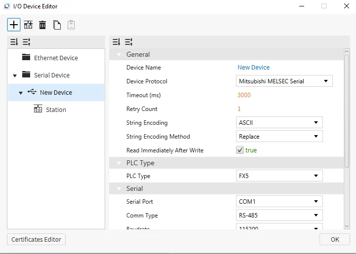
Mitsubishi MELSEC Serial
Canvas supports Mitsubishi MELSEC Serial as a way to connect to devices that support this protocol. Users will be able to choose any of the Mitsubishi PLCs under PLC Type. Users will also need to select the Frame Type for the PLC as well.
Memory Area and Ranges
| Memory Area | Symbol | Digital | Analog | Address Notation | Access |
|---|---|---|---|---|---|
| Input | X | X0000 - X1757 | - | Octal | R |
| Output | Y | Y0000 - Y1757 | - | Octal | R |
| Internal Relay | M | M0000 - M7659 | - | Decimal | R/W |
| Latching Relay | L | L0000 - L7659 | - | Decimal | R/W |
| Annunciator | F | F000 - F107 | - | Decimal | R/W |
| Edge Relay | V | V0000 - V2029 | - | Decimal | R/W No iQ-F No FX5 |
| Link Relay | B | B000 B0EF | - | Hexadecimal | R/W |
| Step Relay | S | S0000 - S4079 | - | Decimal | R/W |
| Timer - Contact | TS | TS000 - TS496 | - | Decimal | R/W |
| Timer - Coil | TC | TC000 - TC496 | - | Decimal | R/W |
| Retentive Timer - Contact | SS | SS00 - SS00 | - | Decimal | R/W |
| Retentive Timer - Coil | SC | SC00 - SC00 | - | Decimal | R/W |
| Counter - Contact | CS | CS000 - CS240 | - | Decimal | R/W |
| Counter - Coil | CC | CC000 - CC240 | - | Decimal | R/W |
| Link Special Relay | SB | SB000 - SB1EF | - | Hexadecimal | R/W |
| Special Relay | SM | SM0000 - SM9979 | - | Decimal | R/W |
| Data Register | D | - | D0000 - D7999 | Decimal | R/W |
| Link Register | W | - | W000 - W1FF | Hexadecimal | R/W |
| Timer - Current Value | TN | - | TN000 - TN511 | Decimal | R/W |
| Retentive Timer - Current Value | SN | - | SN00 - SN15 | Decimal | R/W |
| Counter - Current Value | CN | - | CN000 - CN255 | Decimal | R/W |
| Link Special Register | SW | - | SW000 - SW1FF | Hexadecimal | R/W |
| Special Register | SD | - | SD00000- SD11999 | Decimal | R/W |
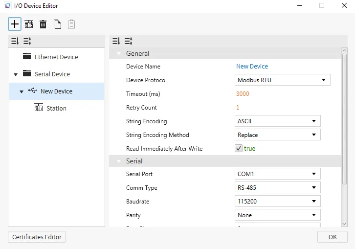
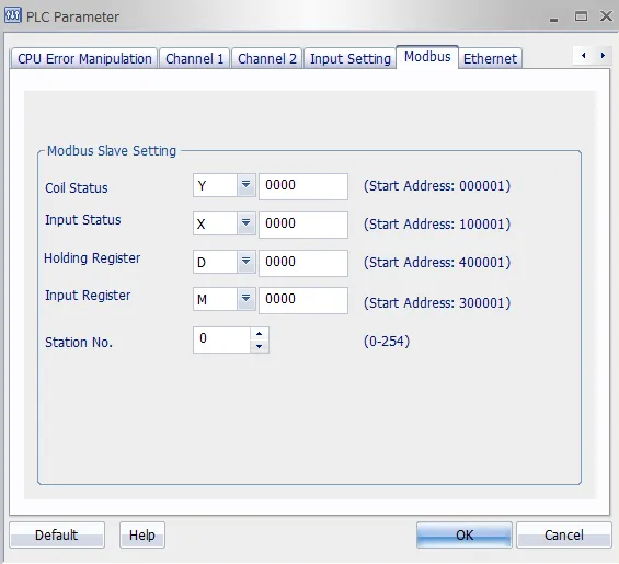
Modbus RTU
Canvas supports Modbus RTU as a way to connect to devices that support this protocol. Users will be able to change the Read Block Tolerance.
Format
- General Format: {Memory Area Symbol}{Address Number}
Memory Area Symbol: refer to the table below. This component is required.- For Coil memory areas
Memory Area Symbol0, the leading 0 cannot be dropped.
- For Coil memory areas
Address Number: index of the memory area to access, represented in decimal notation.- Leading zeros are not required (i.e., 00025 is equivalent to 25).
Memory Area and Ranges
| Memory Area | Symbol | Digital Tag | Analog Tag | Access |
|---|---|---|---|---|
| Coil | 0 | 000001 - 029999 | - | R/W |
| Input | 1 | 100001 - 129999 | - | R |
| Input Register | 3 | - | 300001 - 329999 | R |
| Holding Register | 4 | - | 400001 - 429999 | R/W |
Communication Cable Wiring
| Model | Image |
|---|---|
| Xpanel COM1/COM2 RS-232C | 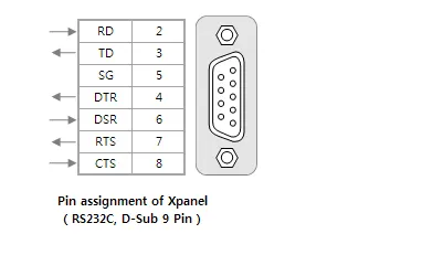 |
| Xpanel COM1 RS-422/485 | 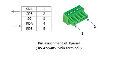 |
The above picture shows the RS-232C and RS-422/485 ports of the Xpanel. Please refer to your device manual for signal descriptions.
For the RS-232C ports, the Xpanel provides the standard DB9 RS-232C pin assignment. Typically, RD, TD, and SG pins are enough to communicate with a general Modbus device.
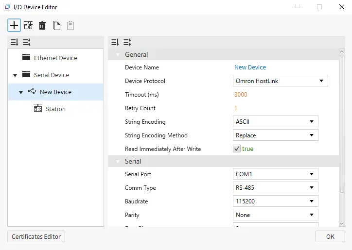
Omron HostLink
Canvas supports Omron Hostlink as a way to connect to devices that support this protocol. No additional settings will appear on the selection of this protocol.
Format
- General Format: {Symbol}{Starting Address}
Symbol: refer to the tables below.- This driver uses some non-standard symbols for the
CounterandTimermemory areas.
- This driver uses some non-standard symbols for the
Starting Address: represented in decimal notation. Does not use leading zeros.
- Expansion Data Notation: E{Bank Number}_{Starting Address}
Bank Number: represented in Hexadecimal notation.- Example: WORD-based tag with
Starting Address149 onBank11 (0xB): EB_00149.
- Example: WORD-based tag with
Starting Address: represented in decimal notation. Does not use leading zeros.
CS1 & CJ1
Memory Area and Ranges
| Memory Area | Symbol | Bit Address | WORD Address | Access |
|---|---|---|---|---|
| Auxiliary Relay | A | A000.00 - A447.15 | A000 - A447 | R |
| A448.00 - A959.15 | A448 - A959 | R/W | ||
| Common I/O | CIO | CIO0000.00 - CIO6143.15 | CIO0000 - CIO6143 | R/W |
| Counter Preset Value | CV | - | CV0000 - CV4095 | R/W |
| Counter Status | CC | CC0000 - CC4095 | - | R/W |
| Data Memory | D | D00000.00 - D32767.15 | D00000 - D32767 | R/W |
| Expansion Data Memory | E | E0_00000.00 - EC_32767.15 | E0_00000 - EC_32767 | R/W |
| Holding Relay | H | H0000.00 - H1535.15 | H0000 - H1535 | R/W |
| Index Register | IR | - | IR00 - IR15 | R/W |
| Timer Preset Value | TV | - | TV0000 - TV4095 | R/W |
| Timer Status | TC | TC0000 - TC4095 | - | R/W |
| Working Relay | W | W000.00 - W511.15 | W000 - W511 | R/W |
CJ2
Memory Area and Ranges
| Memory Area | Symbol | Bit Address | WORD Address | Access |
|---|---|---|---|---|
| Auxiliary Relay | A | A000.00 - A447.15 | A000 - A447 | R |
| A0448.00 - A1471.15 | A0448 - A1471 | R/W | ||
| A10000.00 - A11535.15 | A10000 - A11535 | R | ||
| Common I/O | CIO | CIO0000.00 - CIO6143.15 | CIO0000 - CIO6143 | R/W |
| Counter Preset Value | CV | - | CV0000 - CV4095 | R/W |
| Counter Status | CC | CC0000 - CC4095 | - | R/W |
| Data Memory | D | D00000.00 - D32767.15 | D00000 - D32767 | R/W |
| Expansion Data Memory | E | E0_00000.00 - EF_32767.15 | E0_00000 - EF_32767 | R/W |
| Holding Relay | H | H0000.00 - H1535.15 | H0000 - H1535 | R/W |
| Index Register | IR | - | IR00 - IR15 | R/W |
| Timer Preset Value | TV | - | TV0000 - TV4095 | R/W |
| Timer Status | TC | TC0000 - TC4095 | - | R/W |
| Working Relay | W | W000.00 - W511.15 | W000 - W511 | R/W |
Communication Cable Wiring
| Model | Image |
|---|---|
| RS-232C | 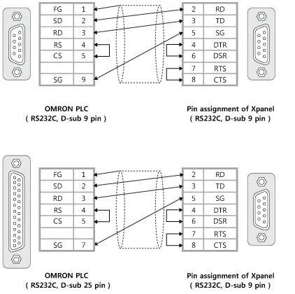 |
| C Series RS-422A | 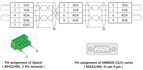 |
| CS/CJ Series RS-422A | |
Panasonic FP7
Canvas supports Panasonic FP7 as a way to connect to devices that support this protocol. No additional settings will appear for the selection of this protocol.
Memory Area and Ranges
| Memory Area | Symbol | Digital | Analog | Address Notation | Access |
|---|---|---|---|---|---|
| External Input Relay | X | X000.0 - X511.F | X000 - X511 | Decimal Hexadecimal | R/W |
| External Output Relay | Y | Y000.0 - Y511.F | Y000 - Y511 | Decimal Hexadecimal | R/W |
| Internal Relay | R | R0000.0 - R2047.F | R0000 - R2047 | Decimal Hexadecimal | R/W |
| Link Relay | L | L0000.0 - L1023.F | L0000 - L1023 | Decimal Hexadecimal | R/W |
| Data Register | DT | DT000000.0 - DT999423.F | DT000000 - DT999423 | Decimal Hexadecimal | R/W |
| Link Register | LD | LD00000.0 - LD16383.F | LD00000 - LD16383 | Decimal Hexadecimal | R/W |
| Timer - Set Value Register | TS | - | TS0000 - TS4095 | Decimal Hexadecimal | R/W |
| Timer - Elapsed Value Register | TE | - | TE0000 - TE4095 | Decimal Hexadecimal | R/W |
| Counter - Set Value Register | CS | - | CS0000 - CS1023 | Decimal Hexadecimal | R/W |
| Counter - Elapsed Value Register | CE | - | CE0000 - CE1023 | Decimal Hexadecimal | R/W |
| Timer - Contact | T | T0000 - T4095 | - | Decimal | R |
| Counter - Contact | C | C0000 - C1023 | - | Decimal | R |
| Pulse Relay | P | P000 - P255 | - | Decimal | R |
| Error Alarm Relay | E | E0000 - E4095 | - | Decimal | R |
| Index Register | I | - | I00 - I14 | Decimal | R/W |
| Unit Memory | UM | UM000000.0 - UM524287.F | UM000000 - UM524287 | Decimal Hexadecimal | R/W |
| Direct Input | IN | - | IN00 - IN62 | Decimal | R/W |
| Direct Output | OT | OT00.0 - OT62.F | OT00 - OT62 | Decimal Hexadecimal | R/W |
| System Relay | SR | - | SR0000 - SR0223 | Decimal | R |
| System Data | SD | - | SD000 - SD255 | Decimal | R |
Yokogawa FA-M3
Canvas supports Yokogawa FA-M3 as a way to connect to devices that support this protocol. No additional settings will appear on the selection of this protocol.

Format
- X, Y Device Addressing Format: {Symbol}{1 Digit for Rack Number}{2 Digits for Slot Number}{2 Digits for Bit Number}
Rack NumberRange: 0 ~ 7Slot NumberRange: 0 ~ 12Bit NumberRange: 0 ~ 63- Example: memory area is X,
Rack Numberis 1,Slot Numberis 3, andBit Numberis 45: X10345
- L Device Addressing Format: {Symbol}{1 Digit for Rack Number}{4 Digits for Memory Address}
Rack NumberRange: 0 ~ 7Memory AddressRange: 0 ~ 1,023- Example: memory area is L,
Rack Numberis 3, andMemory Addressis 45: L30045
Memory Area and Ranges
| Memory Area | Symbol | Digital | Analog | Address Notation | Access |
|---|---|---|---|---|---|
| Input Relay | X | X00201 - X71649 | X00201 - X71664 | Decimal | R |
| Output Relay | Y | Y00201 - Y71649 | Y00201 - Y71664 | Decimal | R/W |
| Internal Relay | I | I0001 - I4081 | I0001 - I4096 | Decimal | R/W |
| Shared Relay | E | E0001 - E2033 | E0001 - E2048 | Decimal | R/W |
| Link Relay | L | L00001 - L71008 | L00001 - L71023 | Decimal | R/W |
| Special Relay | M | M001 - M497 | M001 - M512 | Decimal | R/W |
| Data Register | D | - | D0001 - D5120 | Decimal | R/W |
| Shared Register | R | - | R0001 - R1024 | Decimal | R/W |
| Index Register | V | - | V01 - V16 | Decimal | R/W |
| File Register | B | - | - | - | - |
| Link Register | W | - | W0001 - W1024 | Decimal | R/W |
| Special Register | Z | - | Z001 - Z256 | Decimal | R/W |
| Timer - Relay | TU | TU001 - TU256 | - | Decimal | R/W |
| Timer - Current Value | TP | - | TP001 - TP256 | Decimal | R |
| Timer - Current Value | TI | - | TI001 - TI256 | Decimal | R |
| Timer - Present Value | TS | - | TS001 - TS256 | Decimal | R/W |
| Counter - Relay | CU | CU001 - CU256 | - | Decimal | R/W |
| Counter - Current Value | CP | - | CP001 - CP256 | Decimal | R |
| Counter - Current Value | CI | - | CI001 - CI256 | Decimal | R |
| Counter - Present Value | CS | - | CS001 - CS256 | Decimal | R/W |